Photonic crystals
Photonic crystals (FC) are structures characterized by periodic changes in the dielectric constant in space. The optical properties of FC are very different from the optical properties of continuous media. Due to the periodicity of the medium, the propagation of radiation inside a photonic crystal becomes similar to the movement of an electron inside an ordinary crystal under the action of a periodic potential. As a result, electromagnetic waves in photonic crystals have a band spectrum and a coordinate dependence similar to the Bloch waves of electrons in ordinary crystals.
Under certain conditions, slits form in the FC band structure, similar to the forbidden electron zones in natural crystals. Depending on the specific properties (the material of the elements, their size and the lattice period), both completely frequency–forbidden zones can be formed in the FC spectrum, for which radiation propagation is impossible regardless of its polarization and direction, and partially forbidden (stop zones), in which propagation is possible only in selected directions.
Photonic crystals are interesting both from a fundamental point of view and for numerous applications. On the basis of photonic crystals, optical filters, waveguides (in particular, in fiber-optic communication lines), devices for controlling thermal radiation are being created and developed, designs of lasers with a reduced pumping threshold have been proposed on the basis of photonic crystals.
In addition to changing the reflection, transmission and absorption spectra, metal-dielectric photonic crystals have a specific density of photonic states.
The changed density of states can significantly affect the lifetime of the excited state of an atom or molecule placed inside a photonic crystal, and, consequently, change the nature of luminescence. For example, if the transition frequency in an indicator molecule located in a photonic crystal falls into the forbidden zone, then luminescence at this frequency will be suppressed.
FC are divided into three types: one-dimensional, two-dimensional and three-dimensional.
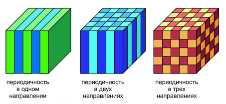
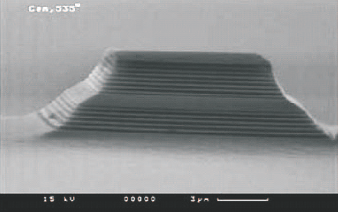
One-dimensional are FC with alternating layers made of different materials.
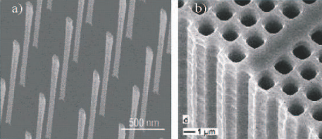
Two-dimensional FC can have more diverse geometries. These include, for example, arrays of cylinders infinite in length (their transverse size is much smaller than the longitudinal one) or periodic systems of cylindrical holes.
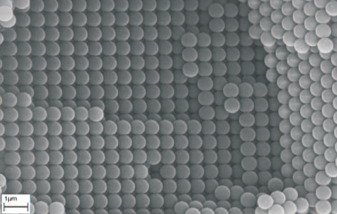
The structures of three-dimensional FC are very diverse. The most common in this category are artificial opals - ordered systems of spherical diffusers. There are two main types of opals: direct and inverse opals. The transition from direct opal to reverse opal is carried out by replacing all spherical elements with cavities (usually air), while the space between these cavities is filled with some material.
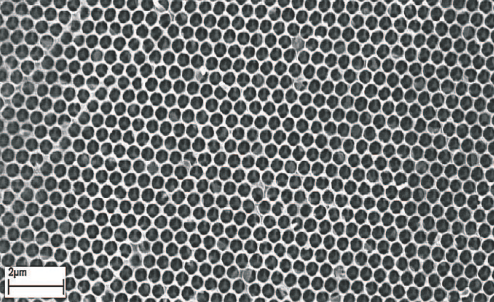
Below is the surface of the FC, which is a straight opal with a cubic lattice based on self-organized spherical microparticles of polystyrene.
The following structure is an inverse opal synthesized as a result of a multi-stage chemical process: self-assembly of polymer spherical particles, impregnation of voids of the resulting material with a substance and removal of the polymer matrix by chemical etching.
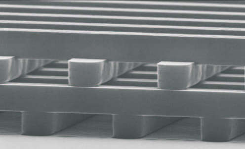
Another type of three-dimensional FC are logpiles structures formed by rectangular parallelepipeds crossed, usually at right angles.
Production methods
The use of FC in practice is significantly limited by the lack of universal and simple methods of their manufacture. Nowadays, several approaches to the creation of FC have been implemented. Two main approaches are described below.
The first of them is the so-called method of self-organization or self-assembly. When self-assembling a photonic crystal, colloidal particles are used (the most common are monodisperse silicon or polystyrene particles), which are in a liquid and, as the liquid evaporates, precipitate in volume. As they “settle” on each other, they form a three-dimensional FC and are ordered, depending on the conditions, into a cubic face-centered or hexagonal crystal lattice. This method is quite slow, the formation of FC can take several weeks. Also, its disadvantages include a poorly controlled percentage of the appearance of defects in the deposition process.
One of the varieties of the self-assembly method is the so-called cellular method. This method involves filtering the liquid in which the particles are located through small pores, and allows the formation of FC at a speed determined by the velocity of the liquid flow through these pores. Compared with the conventional deposition method, this method is much faster, however, the percentage of defects when using it is higher.
The advantages of the described methods include the fact that they allow the formation of large-sized FC samples (with an area of up to several square centimeters).
The second most popular method of manufacturing FC is the etching method. Various etching methods are usually used for the manufacture of two-dimensional FC. These methods are based on the use of a photoresist mask (which sets, for example, an array of hemispheres) formed on the surface of a dielectric or metal and defining the geometry of the etching area. This mask can be obtained using a standard photolithography method, which is immediately followed by chemical etching of the sample surface with a photoresist. At the same time, respectively, in the areas where the photoresist is located, the surface of the photoresist is etched, and in the areas without the photoresist, the dielectric or metal is etched. The process continues until the desired etching depth is reached, after which the photoresist is washed off.
The disadvantage of this method is the use of a photolithography process, the best spatial resolution of which is determined by the Rayleigh criterion. Therefore, this method is suitable for creating a FC with a forbidden zone lying, as a rule, in the near infrared region of the spectrum. Most often, a combination of photolithography with electron beam lithography is used to achieve the desired resolution. This method is an expensive, but highly accurate method for the manufacture of quasi-two-dimensional FC. In this method, a photoresist that changes its properties under the action of an electron beam is irradiated in certain places to form a spatial mask. After irradiation, part of the photoresist is washed off, and the remaining part is used as a mask for etching in the subsequent technological cycle. The maximum resolution of this method is about 10 nm.
Parallels between electrodynamics and quantum mechanics
Any solution of Maxwell's equations \({\bf E}({\bf r},t)\), \({\bf H}({\bf r},t)\) in the case of linear media and in the absence of free charges and current sources can be represented by in the form of a superposition of harmonic functions in time with complex amplitudes \({\bf F}({\bf r},\omega)\), depending on the frequency:
where \(\bf F\) is either \(\bf E\) or \(\bf H\).
Since the fields are real, then \({\bf F}({\bf r},\omega)={\bf F}^*({\bf r},\omega)\), and \({\bf F}({\bf r}, t)\) can be written as a superposition of time-harmonic functions with positive frequency:
Consideration of harmonic functions allows us to move on to the frequency form of Maxwell's equations, which does not contain time derivatives:
where the time dependence of the fields involved in these equations is represented as \({\bf E}({\bf r})e^{-\omega t}\), \( H (r e^{-\omega t}\). We assume that the media are isotropic, and the magnetic permeability is \(\mu=\mu_0\).
Explicitly expressing the field \({\bf E}({\bf r})\), taking the rotor from both parts of the equations, and substituting the second equation into the first, we get:
where \(c=1/\sqrt{\varepsilon_0 \mu_0}\) is the speed of light in the void.
In other words, we got an eigenvalue problem:
for the operator
where the dependency \(\varepsilon({\bf r})\) is determined by the structure in question.
The eigenfunctions (modes) \({\bf H}({\bf r})\) of the resulting operator must satisfy the condition
\({\bf E}({\bf r})\) is found as
In this case, the condition \(\nabla \cdot \left[\varepsilon({\bf r}) {\bf E}({\bf r})\right]=0\) is observed automatically, since the divergence of the rotor is always zero.
The operator \(\hat\Theta\) is linear, which means that any linear combination of solutions to the eigenvalue problem with the same frequency \(\omega\) will also be a solution. It can be shown that in the case of \(\varepsilon({\bf r})=\varepsilon^*({\bf r})\) this operator is Hermitic, i.e. for any vector functions \({\bf F}({\bf r})$ and ${\bf G}({\bf r})\)
where the scalar product is defined as
The Hermiticity of the operator \(\hat\Theta\) implies the realness of its eigenvalues \((\omega/c)^2\). It can also be shown that for \(\varepsilon({\bf r})>0\), the eigenvalues are non-negative, and hence the frequencies \(\omega\) are real.
The scalar product of eigenfunctions corresponding to different frequencies \(\omega_1\ne\omega_2\) is always zero. In the case of equality of frequencies, this is not necessarily the case, but it is always possible to work only with linear combinations of such eigenfunctions orthogonal to each other. Moreover, it is always possible to make a basis from proper orthogonal functions of the Hermitian operator \(\hat\Theta\).
If, on the contrary, we express the field \({\bf E}({\bf r})\) through \({\bf H}({\bf r})\), we get a generalized eigenvalue problem:
in which operators are already present on both sides of the equation (while after dividing by \(\varepsilon({\bf r})\), the operator on the left side of the equation becomes non-Hermitian). In some cases, this formulation is more convenient.
Note that when replacing \({\bf r}^{'}=s{\bf r}\) in the equation with the eigenvalues of the new solution \({\bf H}^{'}({\bf r}^{'})={\bf H}({\bf r}^{'}/s)\) will correspond to the frequency \(\omega^{'}=\omega/s\). This fact is called scalability and has great practical significance. The production of photonic crystals with characteristic sizes of the order of a micron is technically difficult. However, for testing purposes, it is possible to make a model of a photonic crystal with a period and a size of elements of the order of a centimeter, which would work in centimeter mode (at the same time, it is necessary to use materials that would have approximately the same permittivity in the centimeter frequency range as the simulated materials).
Let's draw an analogy of the theory described above with quantum mechanics. In quantum mechanics, the scalar wave function \(\Psi({\bf r})\), which takes complex values, is considered. In electrodynamics, it is vector, and the complex dependence \(e^{-i\omega t}\) is introduced only for convenience. The consequence of this fact, in particular, is that the band structures for photons in a photonic crystal will be different for waves with different polarization, unlike the band structures for electrons.
Both in quantum mechanics and in electrodynamics, the problem of the eigenvalues of the Hermitian operator is solved. In quantum mechanics, Hermitian operators correspond to observable quantities.
And finally, in quantum mechanics, if the operator \(V({\bf r})\) is represented as the sum \(V_x(x)+V_y(y)+V_z(z)\), the solution of the eigenvalue equation can be written as \(\Psi({\bf r})=X(x)Y(y)Z(z)\), that is, the problem splits into three one-dimensional ones. In electrodynamics, this is impossible, because the operator \(\hat\Theta\) "connects" all three coordinates, even if in \(\varepsilon({\bf r})\) they are separated. For this reason, only a very limited number of problems have analytical solutions in electrodynamics. In particular, exact analytical solutions for the band spectrum of FC are found mainly for one-dimensional FC. That is why numerical modeling plays an important role in calculating the properties of photonic crystals.
Zone structure
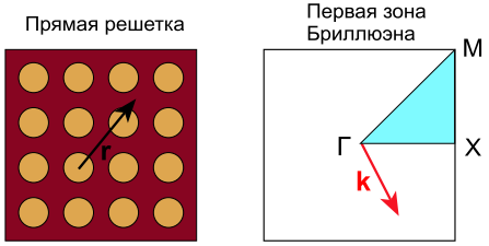
The photonic crystal is characterized by the periodicity of the function \(\varepsilon({\bf r})\):
\(\bf R\) is an arbitrary translation vector, represented as
where \({\bf a}_{1,2,3}\) are primitive translation vectors, and \(m_{1,2,3}\) are integers.
According to Bloch's theorem, the eigenfunctions of the operator \(\hat\Theta\) can be chosen in such a way that they have the form of a plane wave multiplied by a function having the same periodicity as FC:
where \({\bf u}_{\bf k}({\bf r})\) is a periodic function \({\bf u}_{\bf k}({\bf r})={\bf u}_{\bf k}({\bf r} + {\bf R})\). In this case, the values \(\bf k\) can be selected in such a way that they belong to the first Brillouin zone.
Substituting this expression into the formulated eigenvalue problem , we obtain the eigenvalue equation
or
where
Eigenfunctions must be periodic \({\bf u}_{\bf k}={\bf u_k}({\bf r}+{\bf R})\) and satisfy the condition \((i{\bf k} + \nabla) \cdot {\bf u}_{\bf k}=0\).
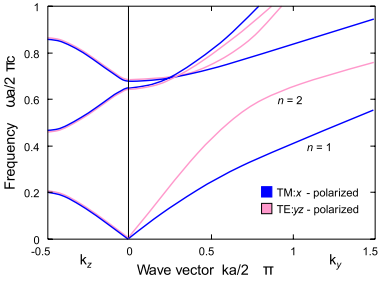
It can be shown that each value of the vector \(\bf k\) corresponds to an infinite set of modes with a discrete set of frequencies \(\omega\), which we will number in ascending order by the index \(n\). Since the operator \(\hat\Theta_{\bf k}\) continuously depends on \(\bf k\), the frequency \(\omega_n\) at a fixed index \(n\) from \(\bf k\) is also depends continuously. The set of continuous functions \(\omega_n({\bf k})\) constitute the zone structure of FC. The study of the FC band structure allows us to obtain information about its optical properties. The presence of any additional symmetry in the FC allows us to limit ourselves to some subdomain of the Brillouin zone, called irreducible. Solutions \(\omega_n({\bf k})\) for \(\bf k\) belonging to this irreducible zone reproduce solutions for the entire Brillouin zone.
Frequency intervals that do not correspond to any modes for any real value of the wave vector are called forbidden zones. The width of such zones increases with an increase in the contrast of the dielectric constant in FC (the ratio of the dielectric permittivity of the constituent elements of a photonic crystal). If radiation with a frequency lying inside the band gap is generated inside such a photonic crystal, it cannot propagate in it (it corresponds to the complex value of the wave vector). The amplitude of such a wave will exponentially decay inside the crystal (an evanescent wave). One of the properties of a photonic crystal is based on this: the ability to control spontaneous radiation (in particular, its suppression). If such radiation falls on the FC from the outside, then it is completely reflected from the photonic crystal. The use of FC for reflective filters, as well as resonators and waveguides with well-reflecting walls is based on this effect.
As a rule, low–frequency modes are concentrated mainly in layers with a high permittivity index, while high-frequency modes are mostly concentrated in layers with a lower permittivity. Therefore, often the first zone is called dielectric, and the next one after it is called air.
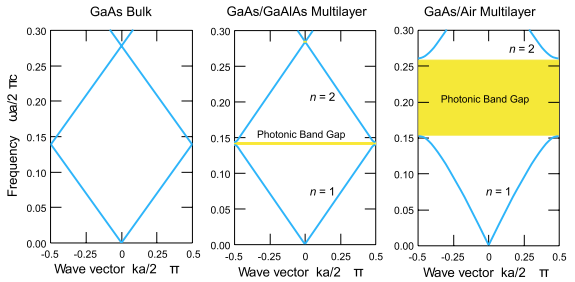
In the case of a FC with dimension less than three, there are no complete forbidden zones for all directions, which is a consequence of the presence of one or two directions along which the FC is homogeneous. Intuitively, this can be explained by the fact that along these directions the wave does not experience multiple reflections required for the formation of forbidden zones.
Despite this, it is possible to create one-dimensional FC that would reflect the waves falling on the FC at any angles.
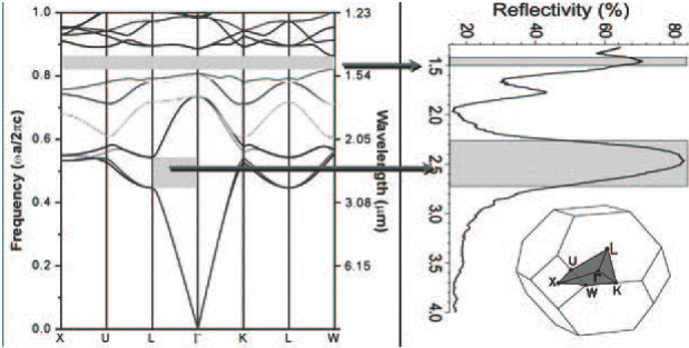
Below is the zone structure of a FC having the geometry of an opal. It can be seen that this FC has a full band gap at a wavelength of about 1.5 microns and one stop zone, with a maximum reflection at a wavelength of 2.5 microns. By changing the etching time of the silicon matrix at one of the stages of manufacturing the inverse opal and thereby varying the diameter of the spheres, it is possible to achieve localization of the band gap in a certain wavelength range. The authors note that a structure with similar characteristics can be used in telecommunication technologies. Radiation at the frequency of the forbidden zone can be localized inside the FC volume, and when the necessary channel is provided, it can propagate virtually lossless. Such a channel can be formed, for example, by removing elements of a photonic crystal along a certain line. When bending the channel, the electromagnetic wave will also change the direction of movement, repeating the shape of the channel. Thus, such a FC is supposed to be used as a transfer node between the emitting device and an optical microchip that processes the signal.
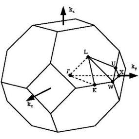
In the case of one-dimensional FC, even the smallest contrast of dielectric permittivity is sufficient to form a band gap. It would seem that for three-dimensional dielectric FC, a similar conclusion can be drawn: to assume the presence of a complete band gap with no matter how small the contrast of the dielectric permittivity is, if at the boundary of the Brillouin zone the vector \(\bf k\) has the same modules in all directions (which corresponds to the spherical Brillouin zone). However, there are no three-dimensional crystals with a spherical Brillouin zone in nature. As a rule, it has a rather complex polygonal shape. Thus, it turns out that the forbidden zones in different directions exist at different frequencies. Only if the dielectric contrast is sufficiently large, then the stop zones in different directions can overlap and form a complete band gap in all directions. The closest to spherical (and thus the most independent of the direction of the Bloch vector \(\bf k\)) is the first Brillouin zone of face-centered cubic (HCC) and diamond lattices, making three-dimensional FC with such a structure most suitable for the formation of a complete band gap in the spectrum. At the same time, for the occurrence of complete forbidden zones in the spectra of such FC, a large contrast of the dielectric constant \(\delta =\epsilon _{max}/\epsilon _{min}\) is required. If we denote the relative width of the gap as \(g=\Delta\omega /\omega _{gap}\), then to achieve the values \(g>5\%\), a contrast \(\delta\geq 9.8\) is needed for diamond and \(\delta\geq 12\) for FCC lattices, respectively. To use forbidden zones in FC spectra in various applications, it is necessary to be able to make the forbidden zone wide enough, bearing in mind that all FC obtained in experiments are not ideal, and defects in the structure can significantly reduce the width of the forbidden zone.
In conclusion, we once again note the similarity of the optical properties of FC with the properties of electrons in quantum mechanics when considering the band structure of a solid. However, there is a significant difference between photons and electrons: electrons have a strong interaction with each other. Therefore, "electronic" problems, as a rule, require taking into account multielectronic effects that greatly increase the dimension of the problem, which often makes it necessary to use insufficiently accurate approximations, while in a FC consisting of elements with a negligibly small nonlinear optical response, this difficulty is absent.
Light sources
A promising direction of modern optics is the control of radiation using photonic crystals. In particular, in the Sandia Laboratory, FC of the log-piles type were studied in order to achieve high selectivity of radiation of metal photonic crystals in the near infrared range, simultaneously with strong suppression of radiation in the middle IR range (<20mkm). In these studies, it was shown that for such FC radiation in the mid-IR range is strongly suppressed due to the presence of a full photon gap in the FC spectrum. However, the quality of the full photon gap decreases with increasing temperature due to increased absorption in tungsten, which leads to low selectivity of radiation at high temperatures.
According to Kirchhoff's law for radiation in thermal equilibrium, the emissivity of a gray body (or surface) is proportional to its absorption capacity. Therefore, in order to obtain information about the emissivity of metal FC, it is possible to study their absorption spectra. To achieve high selectivity of the radiating structure in the visible range ( \(\lambda = 400 - 700\) nm) containing FC, it is necessary to choose such conditions under which the absorption in the visible range is high, and in the IR it is suppressed.
In our works, the change in the absorption spectrum of a photonic crystal with tungsten elements and opal geometry is analyzed in detail when all its geometric parameters change: the lattice period, the size of tungsten elements, the number of layers in the FC sample. The analysis of the effect on the absorption spectrum of defects in FC arising during its manufacture is also carried out.