Plane wave expansion
Eigenmode decomposition is very popular tool to analyze electromagnetic fields inside arbitrary optical systems. In the absence of nonlinearity, any electromagnetic propagation could be represented as a superposition of eigenmodes.
One approach of eigenmodes calculation relies on expanding the eigenmode in series of specially chosen basic functions. Such decomposing leads to finite matrix eigenproblem which can be solved using standard linear algebra.
Different choices of basic functions can be applied correspondingly to considered problem. For example, Chebyshev or Legendre polynomials can be used for finite optical systems, while Fourier series can be used for infinite photonic crystals. Second choice is a core of plane wave expansion (PWE) method that is very suitable for calculation of photonic crystals band structures.
We implemented plane wave expansion (PWE) method as a part of Electromagnetic Template Library (EMTL). Note that EMTL was initially developed mostly for FDTD simulations. Contrary to FDTD, our PWE implementation is much more restricted: currently it does not support calculation of anisotropic or dispersive materials, it is not parallel, etc. However, it can be used for efficient simulation of 2D and 3D photonic crystals.
Below we present illustrative tutorial how to use EMTL for PWE simulations. There is some common syntax with that one used for FDTD, especially concerning how to construct geometry objects, media and media objects.
Bandstructure of 2D photonic crystals
Here we show how to calculate bandstructure of 2D photonic crystal.
To use EMTL for PWE simulations you should include file plane_wave_exp.h to your code
#include "plane_wave_exp.h"
EMTL should be initialized with command line arguments:
int main(int argc, char **argv){
  emInit(argc,argv);
  ...               // your code
  return 0;
}
Function emInit has 3rd optional arguments. You can specify directory for output text files there. This argument is empty strings by default (this means that all files are recorded to directory with your executable file).
The main class for numerical experiment is pwExperiment declared in photonic/plane_wave_exp.h. Lets make object of this class.
pwExperiment task;
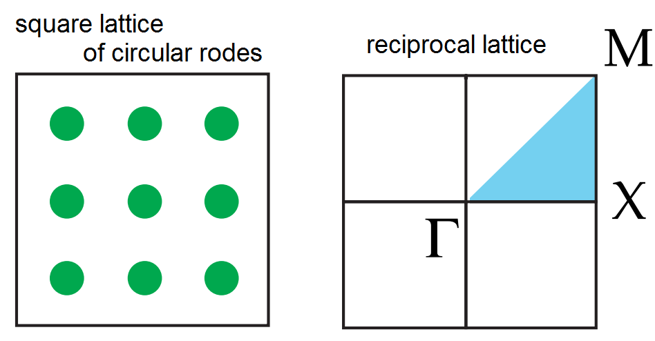
We will calculate band structure for the TM waves inside a square lattice of circular rods (epsilon=11.9, radius = 0.2) in air background.
We define periodic lattice and add circular rod at the central position of the periodic cell:
task.SetLattice(Vector_3(1,0,0),Vector_3(0,1,0));
task.AddObject(emMedium(11.9), GetCylinder(Vector_3(.5,.5,0),Vector_3(0,0,1),.2));
We specify TM polarization (it makes sense only for 2D):
task.SetPolarization("TM");
We are interested in first 10 bands:
task.SetBandsNumber(10);
We will use 50 spatial mesh steps along each dimension. Spatial mesh is used to calculate Fourier representation of inverse dielectric permittivity.
task.SetMeshStepsNumber(50);
We will use \(2\cdot5+1\) plane waves \(\exp{\rm (iGx)}\) along each dimension (5 for G>0, 5 for G<0, and one is G=0). Total number of plane waves is \((2\cdot15+1)^2\).
task.SetPlaneWavesNumber(5);
This is our square lattice and first Brillouin zone.

We calculate eigenfrequencies for a number of wavevectors on the path \(\rm \Gamma-X-M-\Gamma\).
int rsl=10;
for(int i=0;i<rsl;i++)
    task.AddWaveVector(Vector_3(.5*i/rsl,0,0));
for(int i=0;i<rsl;i++)
    task.AddWaveVector(Vector_3(.5,.5*i/rsl,0));
for(int i=rsl;i>=0;i--)
    task.AddWaveVector(Vector_3(.5*i/rsl,.5*i/rsl,0));
task.Calculate();
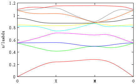
As a result of calculation we get tabular file eig.d with first 10 bands. Table in this file has following columns: number of wavector, three coordinates of wavevector, band frequencies. Open this file by any text editor and see how is it organized.
You can plot bandstructure from this file using popular gnuplot program that can be downloaded from http://www.gnuplot.info.
For example, to plot first 10 bands you should open gnupolt, move to directory with eig.d file using cd command (specify directory name in quotes) and type:
gnuplot> unset key
gnuplot> set ylabel 'a/lambda'
gnuplot> set xtics ("G" 0, "X" 10, "M" 20, "G" 30)
gnuplot> p 'eig.d' u 0:5 w l, 'eig.d' u 0:6 w l, 'eig.d' u 0:7 w l, 'eig.d' u 0:8 w l, 'eig.d' u 0:9 w l, 'eig.d' u 0:10 w l, 'eig.d' u 0:11 w l, 'eig.d' u 0:12 w l, 'eig.d' u 0:13 w l, 'eig.d' u 0:14 w l
This is what you will get:

We hide legend of the plot using unset key gnuplot comand. We also label wavevector numbers 0, 10, 20, 30 by corresponding letters.
In the file bandgaps.d you will find bandgap frequency ranges (if they exist) corresponding to number of specified bands.
Waveguide modes. Supercell technique.
Translation symmetry of photonic crystal can be broken by a defect. Defects may permit localized modes to exist, with frequencies inside photonic band gaps. Using various types of defects one can localize light in the vicinity of a single point (an optical cavity), direct along a particular way (a waveguide), or trap it at a 2D surface. In this section we will illustrate this using example of waveguide formed by linear chain of defect rods inside square lattice of rods from previous section.
To calculate band structures for a photonic crystal with a linear defect we use supercell technique. We assume a periodic structure with a large primitive cell (called a supercell), which includes more than one unit cell. The supercell contains a defect rod (radius chosen differently from the other rods). This supercell is then repeated periodically in a rectangular lattice to form an array of linear waveguides (rows with defect rods) separated by many unit cells of photonic crystal. The effect of coupling between two adjacent waveguides can be made negligible by using a very large supercell.

This is example of applying supercell technique
#include "plane_wave_exp.h"

int main(int argc,char **argv){

  emInit(argc,argv);

  pwExperiment task;

  int super=4;
  task.SetLattice(Vector_3(2*super+1,0,0),Vector_3(0,1,0));
  for(int i=0;i<super;i++){
    task.AddObject(emMedium(11.9), GetCylinder(Vector_3(i+.5,.5,0),Vector_3(0,0,1),.2));
    task.AddObject(emMedium(11.9),GetCylinder(Vector_3(2*super-i+.5,.5,0),Vector_3(0,0,1),.2));
  }

  task.SetPolarization("TM");
  task.SetBandsNumber(50);
  task.SetMeshStepsNumber((2*super+1)*50,50);
  task.SetPlaneWavesNumber((2*super+1)*5,5);

  int rsl=10;
  for(int i=0;i<=rsl;i++)
    task.AddWaveVector(Vector_3(0,i*.5/rsl,0));

  task.Calculate();

  return 0;
}
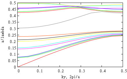
Supercell consists on 2*super+1 unit cells. Defect cell is placed at the center of the supercell. Using this code you can calculate the eigenfrequencies for a number of wave vectors on the path \(\frac{2\pi}{a}(0,0)\) to \(\frac{2\pi}{a}(0,0.5)\).
This is the result for first 15 bands (super=4). One can clearly see waveguide mode which lies in the photonic crystal band gap (grey line).
gnuplot> unset key
gnuplot> set xlabel 'ky, 2pi/a'
gnuplot> set ylabel 'a/lambda'
gnuplot> set xtics
gnuplot> p 'eig.d' u 3:5 w l, 'eig.d' u 3:6 w l, 'eig.d' u 3:7 w l, 'eig.d' u 3:8 w l, 'eig.d' u 3:9 w l, 'eig.d' u 3:10 w l, 'eig.d' u 3:11 w l, 'eig.d' u 3:12 w l, 'eig.d' u 3:13 w l, 'eig.d' u 3:14 w l, 'eig.d' u 3:15 w l, 'eig.d' u 3:16 w l, 'eig.d' u 3:17 w l, 'eig.d' u 3:18 w l, 'eig.d' u 3:19 w l

Eigenmodes spatial distribution
Light in a photonic crystal waveguide can be attenuated if it can couple to propagating (radiation) modes transverse to the axis of the waveguide. This leakage is prevented when the number of photonic crystal unit cell on both sides of the waveguide is large enough. If the guided mode exists below the light line it cannot couple to the radiation field and it is not leaky.
The example below calculates band structure and field distribution for the photonic crystal with a linear defect and air cladding layers.
#include "plane_wave_exp.h"

int main(int argc,char **argv){

  emInit(argc,argv);

  pwExperiment task;

  int super=15;
  int super_air=12;
  task.AddObject(emMedium(11.9),GetCylinder(Vector_3(super+.5,.5,0),Vector_3(0,0,1),.12));
  for(int i=0;i<super;i++){
    if(i>=super_air){
      task.AddObject(emMedium(11.9),GetCylinder(Vector_3(i+.5,.5,0),Vector_3(0,0,1),.2));
      task.AddObject(emMedium(11.9),GetCylinder(Vector_3(2*super-i+.5,.5,0),Vector_3(0,0,1),.2));
    }
  }

  task.SetPolarization("TM");
  task.SetBandsNumber(50);
  task.SetMeshStepsNumber((2*super+1)*50,50);
  task.SetPlaneWavesNumber((2*super+1)*5,5);

  int rsl=10;
  for(int i=0;i<=rsl;i++){
    string str="";
#    if(irsl-2)
      str="0.4";
    task.AddWaveVector(Vector_3(0,i*.5/rsl,0),str);
  }

  task.AddBandDistribution(7);
  task.AddBandDistribution(19);

  int size=10;
  task.AddDetectorSet("f",0,Vector_3(2*super+1,size,0),iVector_3(10*(2*super+1),10*size,1));

  task.Calculate();

  return 1;
}
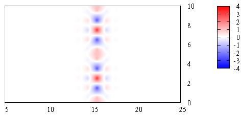
We calculate eigenmode spatial distribution for wavevector 0.4, bands 7, 8. For this purpose we use function AddBandDistribution (this function can be called more than one time for different bands). We use second optional parameter of function AddWaveVector to mark wavector at which we want to calculate spatial eigenmode distribution. Default value of this parameter is empty string "" (spatial distribution will not be calculated).
Function AddDetectorSet specifies points (detectors) where we want to calculate eigenmode value. Syntax of this function is the same as syntax used for FDTD simulations. First parameter of AddDetectorSet is detectors name (“f” in our case). This name will be used for names of files associated with detectors. Next three parameters specify 3D grid where detectors are placed, namely, two opposite corners of the grid and number of grid steps along three directions.
As a result of calculation we get files DetectorName_WavevectorName_Bandnumber.d. These files contain tabular data in the format x - y - z - Re(field) - Im(field) In our 2D case of TM polarization, field corresponds to z-component of electric field E. Files with field spatial distribution can be plotted by gnuplot.
gnuplot> set pm3d interpolate 2,2
gnuplot> set view 0,0
gnuplot> cmax=4
gnuplot> set palette defined (-cmax 'blue', 0 'white', cmax 'red')
gnuplot> set cbrange [-cmax:cmax]
gnuplot> sp [5:25] 'f0.4_7.d' u 1:2:4 w pm3d

In this example we plot eigenmode corresponding to band 7 at wavevector 0.4. This is waveguide mode (it also can be seen from results for bandstructure). We choose gnuplot parameter 'cmax=4' for better color resolution (for other eigenmodes optimal value of cmax could be different). We plot real part of eigenmode \({\rm Re}({\bf E})\). Electric field in time is a combination of real and imaginary parts: \({\rm Re}({\bf E}\exp{(i\omega t)})\).